Floorplanning Large FPGAs
September 2011
For well over a decade all but the most ambitious FPGA designs were fitted automatically by your FPGA vendor's place and route (P&R) software. Occasionally a high performance DDR or DSP macro was in need of location constraints, particularly to tie it to IO resources, but for the most part mainstream design practice let software handle all aspects of the P&R effort. Indeed, until very recently it was generally enough to write a good set of timing constraints, and iterate over placement seeds a few times to meet timing. This is probably the way things should be, since computers are usually much more diligent in optimising logic placement across innumerable competing constraints than us humans are.
However, the technology scaling trends so evident in ASIC designs when they shrunk below 180nm are now also hitting the FPGA world several years on. Chief among these trends is the growing disparity between raw logic gate speed and routing speed. As the former improves at a steady rate, the latter remains almost stuck in yesteryear. The effects of massive density growth, and to a lesser extent, die growth only exacerbate the routing problem.
To make matters worse, P&R software now faces a greater challenge because small mistakes in placement are now proportionally more costly in timing QoR than ever before. When it takes a few clock cycles to cross the die there are no longer the kind of margins of a few years ago. It seems that both of the major FPGA vendors have done little to regain ground in P&R effectiveness of increasingly large designs. Their silicon now routinely outscales their software; it's no longer possible to even use all that silicon unless you address P&R issues!
Floorplanning Concepts
For smaller designs, say less than 25% of device capacity, or designs operating at low, sub-100MHz frequencies automatic P&R may be all that's required. Indeed, most P&R tools have reasonably effective placement algorithms for designs with the luxury of space. But in the real world we want our FPGAs to not only be packed to the brim, but run at speeds demanded by modern protocols and the promise of that fast silicon. In these cases, your only option may be to floorplan the implementation.
But before you do anything further, check that your timing closure issues are indeed candidates for floorplanning. You may need to consider floorplanning if any of the following occur:
- Post P&R timing has many and large cases of negative slack, which are not reflected in the estimated timing analysis of post-synthesis netlists. In other words, what appears to be adequately pipelined, fast logic still cannot meet timing.
- The majority of your negative slack timing paths are dominated by routing delays. Typically, look for paths where routing constitutes 75% or more of the overall path delay.
- Many of your failing paths involve closely-coupled logic (such as adder carry chains) that appear to be placed very loosely with respect to each other. This is evidence of your design hierarchy being obliterated.
- Timing may be met on occasions, but never with any consistency. If you're finding yourself trying upwards of 5 placement seeds (or cost tables) to meet timing, you may have significant placement concerns.
- P&R run-times are measured in the tens of hours for designs with less than 70% device utilisation, regardless of whether timing was met or not.
It should be noted that floorplanning is not hand placing your logic. In this respect, the location constraints of the specialised IO block is not really floorplanning either. We always want to avoid manual placement of logic because such placements are fragile: they can break when the design changes; they can break when P&R runs with different simulated annealing constraints; they are not portable across devices, even in the same family.
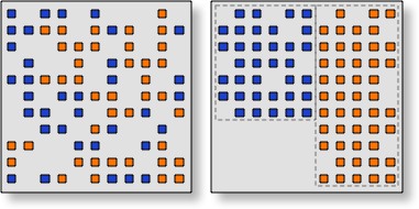
Illustration of floorplanning's effect on placement. Left: blue and orange logic placed automatically. Right: logic floorplanned into blue and orange placement blocks.
Floorplanning can be best described as the introduction of placement constraints on the logic. A placement constraint simply communicates a rule such as a recommended placement region for a group of logic elements. It's still up the P&R tool to actually place the logic while satisfying the constraints. The benefit of constraining placement is simply illustrated by the figure. Originally, automatically placed logic elements (shown blue and orange to distinguish them by function) are spread haphazardly across the FPGA. Worst-case routing between elements can be very large due to the spread in placement. The act of floorplanning constrains placement to within tighter placement blocks (shown with dotted line outlines). The floorplanned placement keeps functionally related logic close to each other, thus minimising routing delays.
As added benefits, the floorplanned logic will typically reduce the time taken in P&R, as well as increasing maximum utilisation of the device. So it may be worth considering floorplanning even when a design meets timing, but takes long run-times in fitting. This will be especially true for designs of 100,000+ LUTs (million-plus gate equivalents), increasingly becoming prevalent with newer FPGAs.
The remainder of this article will look at a design flow for floorplanning, and examine the issues to be expected. A good starting point for floorplanning Xilinx designs is their Floorplanning Methodology Guide, which is aimed at PlanAhead users. Altera users should consult the Chip Planner manual for the Quartus software.
Getting Started
Unless you're very lucky or experienced, your first attempts at floorplanning a new design may well leave you bitterly disappointed as your initial efforts actually degrade timing! But, "I thought it was supposed to get better with constraints!" Yes, and no. The main problem frequently introduced by your first floorplan is overconstraint. That is, logic that was once freely placeable now becomes constrained, which exposes previously unseen critical communication paths. Automatic P&R would have previously optimised such placements to keep these routes under a clock cycle, but now you have intervened to the detriment of those paths.
This should remain as a reminder that poor floorplans can introduce stubbornly unresolvable timing issues, while even good floorplans expose almost every timing weakness in the design. Your task in a successful floorplan design flow is to eliminate those weaknesses through a process of successive refinement.
In their guides, FPGA vendors dwell on preparing a design for floorplanning. Their advice is invariably correct, as time spent at the RTL level can greatly improve chances of timing closure during floorplanning. Indeed, in some cases, it may be simply impossible to meet timing unless structural issues are dealt with beforehand. The preparation is as follows.
Hierarchy Planning
Ideally, floorplanning begins before any RTL is written. You would normally decompose a design along functional lines, with your hierarchy of blocks reflecting the functional relationships. While you may still do this, be aware that particularly deep nesting of hierarchy can be at odds with the practical limitations of floorplanning software (and your patience) to group blocks into a placement region. For example, a pair of blocks may need to communicate via large net bundles, yet they appear in quite disparate parts of the functional hierarchy.
It is always better to consider both functional relationships and inter-block communications when designing the hierarchy. Frequently, a dataflow diagram can be used to assist in creating a draft paper and pencil floorplan. The floorplan regions do not necessarily align 1:1 with hierarchy, but such is the ideal. You would aim to make each floorplan block as large as either you can consistently meet timing with, or as large as its functional hierarchy allows.
With some experience on a particular device (and speed grade) it becomes clear what block size will lead to block-level timing closure for a given clock frequency. However, do not expect more than 10,000 LUTs in any single block. Use of many, smaller blocks may meet timing at the block level, but expose dataflow issues due to overconstraint if those smaller blocks have mutually dependent communications.
Finally, consider which of your logic is deliberately not floorplanned. The best candidates for this are very low frequency logic, and logic that is naturally constrained by IO locations.
Dataflow Planning
As noted above, floorplanning is ultimately concerned with bounding data communications delays. A feasible floorplan has to limit the distance a signal travels in any timing arc. This means that layouts that result in large fanouts radiating from a single block will make timing different. Similarly, layouts that physically separate communicating blocks are less successful than layouts that place logic in the same sequence as the data flows. Indeed, if possible, aim to use nearest-neighbour communications wherever possible. Logic block pipelines, rings, and star topologies are natural examples of such communications.
A practical example is a homogeneous array of processor blocks whose final results would normally be MUXed into a master control (consumer) block. The MUX is the logical means of selecting a processed result from the array, but the routing of all the result buses to a central location places a significant burden on P&R. A more floorplan-friendly architecture has redesigned processor blocks that pass data in shift register fashion from one block to its nearest neighbour, with the master control block connected to the last processor in the chain. Provided that time can be found to operate result shifting, this design is only marginally more complex, but almost unlimited in scalability for floorplanning.
Plan for buffer elements whose function is simply to break up timing arcs, moving data from A to B via registers. Such blocks are not functionally necessary, but in the real world of floorplanning they can become vital elements in the solution. Negative slacks in even normally conservative flop-to-flop paths are indicative of this situation. However, be warned that automatic shift register inference can, in some circumstances (Xilinx's XST is notorious for this), absorb your pipeline registers into one of the end-point blocks—not quite what you had intended. Timing analysis or study of the netlist will quickly show the absence of registers in this case. A reliable hack here is to force the buffer register to be reset, which disables shift register inference.
Clock Domain Planning
The crossing of clock domains can offer floorplan surprises. A common scenario involves a supposedly relaxed timing signal in a slow clock domain appearing to fail timing at its capture flop. Almost invariably the capture flop is clocked at a higher synchronous frequency, cutting the data required time to the smaller, more pessimistic clock period. Deliberately operating block interface registers at the slower clock frequency of the launch flops preserves the relaxed timing of the interface signals, since it moves the slow to fast data transfer problem to within the floorplan block, where the tighter intra-block routing can cope with it.
A special case is the routing of resets—be they synchronous or asynchronous. Route the master reset signal in the slowest, synchronous clock domain available (say, at one half or one quarter of the client block frequencies), and register a local copy of this reset in each floorplanned block. Copy the local reset to one more register in the fast clock domain, which will be constrained in its placement, and fanout the high-speed reset (possibly via cloned registers) to local logic.
If possible, keeping inter-block signal transfers in a common clock domain is preferred. This doesn't mean that all interfaces to a block must share a common clock, only interfaces between interacting blocks. For instance, blocks A and B might share one clock domain, while blocks A and C might share a different clock domain.
Block Interfaces
It's still good design practice to at least register every block output. But where floorplanning is concerned, it's even better to also register every input and output at the boundaries of floorplan blocks. This gives P&R the maximum possible slack in routing between blocks, which gives you the most flexibility in planning block placements. But don't get too zealous about it either: a single LUT delay on inputs or outputs adds less than one hundred picoseconds, but might address a critical performance need on interfaces.
Since floorplanning constrains placement, it can also add to routing congestion between blocks. To this end, it is always sound practice to reduce the width of net bundles on interfaces to absolute minima. For example, faced with sending data over a 128-bit bus, consider sending it over 32-bits of bus in four clock cycles. Fewer nets to route result in more consistent timing results. Similarly, avoid 1-to-N fanout situations by replicating the N specific outputs, using synthesis pragmas if necessary for logic preservation.
Feasibility Study
At this point we need to estimate—based on past synthesis or fitting reports—the resources requirements of your draft floorplan. Certainly, P&R will most likely not succeed unless some "white space" remains in which to place individual logic elements and route them. As a rule of thumb, do not expect any individual floorplan block to pack appreciably tighter than 90% slice/LUT utilisation. For especially fast blocks, keep utilisation in the low 80%'s. While simply dividing the total LUT count by 80% may provide a gross device resource count, this ignores the inevitably wasted space that appears around packed rectangular blocks.
Ideally, you should aim to draw a candidate floorplan out on paper, or use a floorplanning tool, such as Xilinx PlanAhead, to trial the layout with respect to the (usually) square array of logic elements. The most P&R-efficient block shapes are square, but rectangles no less skinny than 1:5 will usually work fine as well. Also, remember to account for the resources of any unfloorplanned logic as additional utilisation. The trial layout should never overlap blocks, but blocks can abut if necessary. Play with the layout until you are satisfied that it can be accommodated on the device. Otherwise, you will need to find ways of shrinking the design or arranging a tighter packing. Even if all goes well, this is merely preparation, since the P&R tools have not had a chance to prove effectiveness of the floorplan yet.
In a homogenous sea of gates you might be ready to start floorplanning now. But the reality is that many of your floorplanned blocks will have peculiar resource requirements that even further constrain what is feasible. The usual culprits are blocks that are heavily reliant on either embedded block RAM or DSP resources. Since these specialised resources are typically scattered evenly and sparsely across the die, they can quickly turn a small block into one that spans vast regions of the device, albeit at rather low logic utilisation. You may wish not to floorplan such blocks because of their area, but routing to all the distant resources will be very difficult for P&R software. Constrain such blocks to enclose 100% of the special resources required, but don't expect other blocks to overlap unless you specifically group other parts of the design's hierarchy in with the floorplan block. In some cases it can be worth redesigning blocks that make heavy use of special resources to achieve better packing density and better QoR. For example, replacing a four-DSP complex multiplier by an equivalent three-DSP formulation would shrink a block performing complex maths.
Iterating Over the Floorplan
If you take a big-bang integration approach to floorplanning, you may well be fighting timing violations on many fronts at once, and probably introducing even more timing fails as you jiggle blocks around from one trial to the next. An incremental approach, on the other hand, confirms feasible options before progressing to larger builds; it also speeds the workflow because the early builds have less logic to P&R.
Starting from the rough draft layout of your feasibility plan (earlier), build up the floorplan in stages. As your overall design may not be buildable in pieces, it may be necessary to stub out unused blocks for the early iterations. Such stub blocks are simply tiny fakes that present the correct interfaces, but don't allow synthesis to accidentally optimise away the blocks being floorplanned. Typically, input-side logic or core logic can be introduced before middle and outer blocks. You might evolve your floorplan in three or four iterations, depending on how interdependent blocks are.
At each iteration, aim for achieving a clean timing result at P&R. Address each case of negative slack before moving on. Commonly, addition of pipelining, splitting critical paths, logic cloning, and any of the usual RTL-level optimisations may be necessary. Pay particular attention to any overlooked planning issues (such as interfaces and clocking) that were discussed above.
The best floorplans tend to be compact, spread over as little of the die as possible. This is hardly surprising, as we're aiming to minimise routing delays for as much of the design as possible. In many cases, regularity goes hand-in-hand with compactness. Arrays of replicated structures are frequently ideal layouts.
Only Floorplan What's Necessary
It is unlikely that you will need or want to floorplan the entire design. Slower logic, such as PCI local buses or Ethernet, will be naturally constrained by IO locations, and will pose few risks to timing closure. Such unfloorplanned logic may, in fact, be placed automatically within the blocks specifically set aside for floorplanned logic. This is rarely a problem, and helps to improve utilisation of otherwise poorly utilised regions.
By default, floorplanning tools constrain physical blocks to be inclusive of logic. That is, the hierarchy being constrained must be placed within the given bounds, but unfloorplanned logic may coexist in the same bounds if possible. However, you should be able to give floorplan blocks exclusivity attributes, which prevents all but specified logic being placed in the block. This option should not be exercised unless very high utilisation or very fast clocks prove troublesome in P&R.
A particularly important use of unfloorplanned logic is pipeline registers inserted between blocks to break long timing paths—say, between distant, separated blocks on the device. Allowing the P&R software automatic placement of such registers can often produce more optimal results than a manual placement.
Concluding Thoughts
Progressing from the first, probably disastrous, results to a final floorplan that meets timing can be both a very satisfying, but time consuming experience. Seemingly incurable P&R problems can be attacked with floorplanning; at the very least, your Fmax should be significantly improved and run times minimised.
It is particularly important to remember that our ability to create good placements is largely dependent on iteration and patient refinement. After all, if it was easy, software would be doing it properly already?